Monday, December 15, 2008

The Latest Thin-Film Processing System from Advanced Solar Photonics

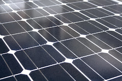
Advanced Solar Photonics, (ASP), a developer of laser scribing, laser marking, laser cutting, edge deletion & edge isolation laser systems for the solar industry, has started promoting the FL600, a thin-film solar cell processing system.

The FL600 is capable of direct fiber laser patterning on indium tin oxide (ITO), TCO, CTO, anti-reflective coatings on glass and PET plastic film as used in the flat panel display industry. ASP is utilizing this proven technology for solar applications. The FL600 is able to accommodate the conventional 2’ x 4’ size solar panels and is also available in a larger format with similar technology for the larger size solar panels. Additionally, the FL600 has an optional conveyor to assist in the maneuverability of fragile solar panel materials for continuous manufacturing.

The FL600 is an easy to use machine and is ideal for high-tech applications such as edge deletion or isolation,” said Kristen Breunig, Market Manager for ASP. “ASP is privileged to have this technology which has been developed and utilized by our parent company, Fonon Technology International, in the flat panel display for over 15 years.“

As the solar industry moves towards the abundant and cost effective thin-film panels, it is increasingly necessary to develop equipment capable of processing the largest solar panels possible. Although thin-film is the most inexpensive, it is also is the least energy efficient, leading to the exponential increase in substrate sizes. Researchers have found that a ten times increase in substrate area only results in a 2.5 times increase in equipment costs. Advanced Solar Photonics not only offers standard equipment for marking, etching, scribing and edge isolation of smaller silicon solar panels but is now developing systems and equipment to process up to an eight foot (G8) thin-film solar panel.

ASP is located in a 318,000 square foot headquarters in Lake Mary, Florida employing an international team of technology driven professionals. Reaching out to the photovoltaic industry, ASP strives to lower manufacturing costs utilizing proven patented technology geared to improve and lower the cost per kilowatt. This technology is applicable to both the silicon and thin-film processes.

What can Advanced Solar Photonics do for you today?

Proven Sales and Marketing Experts to Lead Advanced Solar Photonics

Lake Mary, FL. – Advanced Solar Photonics, (ASP),a developer of laser scribing, laser marking, laser cutting, edge deletion & edge isolation laser systems for the solar industry, announced today it has appointed Edgardo Rodriguez to Vice President of Sales and Marketing and Kristen Breunig to Market Development Manager. In their new roles, they will continue to strengthen the company's ties to the photovoltaic industry.

As vice president of sales and marketing, Edgardo will be responsible for new client acquisition, account development and overseeing the marketing team. Kristen is responsible for ASPs’ overall marketing efforts.

“With Edgardo and Kristen heading up our solar industry division, said Demitri Nikitin, founder and CEO of Advanced Solar Photonics, “their skills and talents will result in a more effective and efficient sales and marketing push that will propel Advanced Solar Photonics through the coming years.”

Prior to joining Advanced Solar Photonics, Edgardo has been involved in sales and marketing for equipment in High Tech industry for the past 15 years, managing Far East and Latin America regions. He received electronics training from Keesler Tech, and a Physics degree from the University of Utah. He has been managing sales for laser equipment manufacturing since 2005.
Kristen studied market development at the University of Central Florida where she received her Bachelor’s degree. She studied advertising at Mindcomet before starting work with Laser Photonics. At Laser Photonics she has played an integral role in developing the company and with that experience she will began development of ASP.


About Advanced Solar Photonics (ASP)
ASP is located in a 318,000 square foot headquarters in Lake Mary, Florida employing an international team of technology driven professionals. Reaching out to the photovoltaic industry, ASP strives to lower manufacturing costs utilizing proven patented technology geared to improve and lower the cost per kilowatt. This technology is applicable to both the silicon and thin-film processes.

For additional information on ASPs’ product technology for the photovoltaic industry, please contact a representative at 1-407-829-2613, or visit http://www.advancedsolarphotonics.com/.

New Bright Light in the Solar Industry


Lake Mary, FL. - And then there were two. Laser Photonics has split off its solar division into a separate entity named Advanced Solar Photonics (ASP). The new sister company specializes in the latest generation of laser technology and laser products tailored to applications in the solar panel fabrication industry.

Founded in 2001, Laser Photonics develops high quality reliable industrial laser solutions that are both simple to operate and cost effective. Laser Photonics Fiber and CO2 Laser Systems are ideal for applications such as marking, cutting, engraving, scribing and other material processes.


Having an advantage over its counterparts due to the longevity of Laser Photonics, its sister company, ASP, provides a turnkey solution for solar manufacturing developing systems for laser marking, scribing, and edge deletion in the solar industry. Additionally, ASPs’ proven patented technology is applicable to both the silicon and thin-film processes.

"Today, solar power is thought to be the cleanest, most reliable and plentiful energy resource available, though it's potential has not yet reached fruition, said Demitri Nikitin, ASP founder and CEO. “We see great opportunities in this growing industry."


ASP is located in a 318,000 square foot headquarters in Lake Mary, Florida employing an international team of technology driven professionals in order to address the needs of the PV solar manufacturers utilizing proven patented technology applicable to both the silicon and thin-film processes.

For additional information on ASP product technology applicable to both the silicon and thin-film processes, please contact a representative at 1-407-829-2613, or visit http://www.advancedsolarphotonics.com/.

Tuesday, December 9, 2008

SunPanels

The highlights of Advanced Solar Photonics SunPanels:

Generation 8 SunPanel - Provides 8 times more power from one panel than competition.

Increased Power Output - Frameless design delivers 8.2% overall power gain over conventional design only on size and geometry.

Increased Efficiency - Dramatic efficiency increase with implementation of E2 process. (Patent pending)

Active Layer contamination free continues manufacturing process is the key to the PV cell efficiency.

Front Glass Substrate - Low E, laser-strengthened laser cut, (see patent information) UV resistant glass substrate.

Back Cover Glass Multi-layer, hurricane proof grade, thin glass laminated design from aerospace and modern security glass technology.

All Glass Components manufactured with patented Zero Width Laser Cutting Technology™ providing 4-5 times stronger and defect free edges to withstand extreme Day/Night temperature changes in the hash desert environments ensuring 25+ year of long term SunPanel™ module stability.

Laminate Material – Liquid, UV curable glass bonding agent converts multi-layer glass stack into a monolithic, weather and shatter proof, sealed photovoltaic device. External Connection accomplished with a single junction box, reducing the installation time and copper wire consumption.

SunPanels™ manufactured in a high throughput continues automated line.

Installation – more than 17% savings on installation costs

SolarTower

The SolarTower™ is Advanced Solar Photonics’ commercial photovoltaic solution for solar energy by commercial and industrial businesses. The Solar Towers™ design allows for the highest amount of energy produced with the smallest footprint. This new design incorporates Advanced Solar Photonics’ SunPanels™ by mounting them to an innovative modular pole design allowing for ingenious utilization of space. Our SunPanels™ can be mounted strategically around your facility without the use of conventional mounting on roofs.


  • Generates approximately 4 kW per SolarTower™
  • Automated Sun Following allows the SolarTower™ to move with the suns motion, maintaining constant solar exposure
  • Multiple SunPanels™ can be added for increased power generation
  • Small plot size needed for installation.
  • Meets state requirements for solar energy incentive programs.
  • Modular design of base to accommodate additional panels as needed

Thin-Film Industry Equipment


The system needed in the thin-film industry will need a high accuracy and precision rate for the large G8 sized panels. ASP’s laser solution will provide the accuracy needed for maintaining the cut along a straight line, precision for making sure this straight line is at the chosen location and finally resolution to ensure the laser scribe line is generating the proper depth. The strict requirements and high processing speeds have made it impossible to use any other method than laser technology

Silicon Solar Industry Equipment

Advanced Solar Photonics also offers customized solutions for the solar industry. Each system can be designed to meet a company’s individual manufacturing requirements to optimize yield. Systems can also be introduced into an existing line or be fully automated to decrease damage due to substrate handling. The systems for the silicon industry are used for wafer dicing, marking and edge isolation. Further equipment is needed for loading and unloading, backlit inspection, and ASP is prepared to fully automate this within the existing product lines.


Our Solar Line

Advanced Solar Photonics (ASP) is focused on providing innovative, latest generation laser systems, products, processes and technologies. Its SunPanels™ and laser systems for solar manufacturing are of the highest quality, durability and are proven to lower manufacturing costs.

Advanced Solar Photonics is your partner in the solar industry. Whether you’re looking to purchase our thin-film SunPanels™ or our innovative laser systems to manufacture solar panels, Advanced Solar Photonics is here for you.

ASP’s Thin-Film SunPanels™
Using lean manufacturing principles, SolarFab,™ produces large G8 to G10 size thin-film SunPanels,™ featuring a 2-3% increase in efficiency and a lower manufacturing cost. SunPanels™ are of the highest quality in reliability and durability with the ability to withstand strong weather conditions and meet any stringent requirements.

ASP’s Laser Systems for Solar Manufacturing
Based on ASP’s exclusive technology and patents, ASP can provide equipment to the solar industry with the most advanced technology for laser scribing, marking, cutting, etching, edge deletion and edge isolation. ASP laser system technology is applicable to both the silicon and thin-film processes.

The SolarTower™
The SolarTower™ is Advanced Solar Photonics’ commercial photovoltaic solution for solar energy by commercial and industrial businesses. Incorporating ASP’s SunPanels™ onto a innovative modular pole design, the SolarTower™ design allows for the highest amount of energy produced with the smallest footprint.

More About Advanced Solar Photonics


Laser Photonics Sister Company to Advanced Solar Photonics


Advanced Solar Photonics is a sister company of Laser Photonics. Laser Photonics serves as the research and development lab for Advanced Solar Photonics, continually working toward improved technology and innovative ideas to help its companies grow and develop new products.


Laser Photonics developed the capabilities for scribing, marking, edge isolation, cell sorting, cell inspection and general automation. The accuracy, precision, resolution, dependability, accessibility and overall superiority of Laser Photonics technologies and products are proven to be consistent and repeatable throughout the years. Having been a key factor in the flat panel display, solar and semiconductor industries for over 10 years, Laser Photonics has provided a proven solution to the solar industry for material processing.


In order to strengthen its position in the worldwide market, Laser Photonics has recently expanded its production site in Lake Mary, FL to encompass a 312,000 square foot facility with a dedicated 58,000 square foot application and research lab.

Solar Industry Time Line

1954
Photovoltaic technology is born in the United States — the first solar cell capable of generating enough power from the sun to run everyday electrical equipment. A silicon solar cell with 6% efficiency and later, 11% efficiency is developed.

1960
Photovoltaic cells reach 14% efficiency.

1970
A significantly less costly solar cell is designed, bringing the price down from $100 per watt to $20 per watt. Solar cells begin powering navigation warning lights and horns on offshore gas and oil rigs, lighthouses, and railroad crossings.

1977
Total photovoltaic manufacturing production exceeds 500 kilowatts; 1 kilowatt is enough power to light about ten 100-watt light bulbs.

1985
Researchers at the University of South Wales break the 20% efficiency barrier for silicon solar cells.

1986
The world's first commercial thin-film module is released.

1991
Fonon patents Zero Width laser Cutting Technology as the method that scribes glass on the molecular level causing no micro cracks and increasing the strength.

1998
The Blackstar is built for the dicing silicon wafers and using Fonon’s patented method for wafer dicing.

1999
The FL 600 is created for patterning and coating removal sold to the Flat Panel Display industry.

2007
Advanced Solar Photonics was created with a mission to make the cost per kilowatt of solar panels more affordable by lower manufacturing costs using patented technology, experience and innovation in laser solutions for thin-film and silicon solar panel processing.

2007
Advanced Solar Photonics sells to its first customer

Thin-Film Technology

As the solar industry moves towards the abundant and cost effective thin-film panels it is increasingly necessary to develop equipment capable of processing the largest solar panels possible. Although thin-film is the most inexpensive it is also is the least energy efficient. This has lead to the exponential increase in substrate sizes. Researchers have found that a ten times increase in substrate area only results in a 2.5 times increase in equipment costs. Advanced Solar Photonics not only offers standard equipment for marking, etching, scribing and edge isolation of smaller silicon solar panels but is now developing systems and equipment to process up to an eight foot (G8) thin-film solar panel.

Silicon Technology


The most energy efficient solar panels are produced from Silicon. Silicon is also said to be the predominate material used in solar production for the next 10 years for generation 1 panels. There are two types of crystalline silicon typically used in the industry. The first is monocrystalline, produced by slicing wafers from a high-purity single crystal boule and the second is multicrystalline silicon, made by sawing a cast block of silicon first into bars and then wafers. The main trend in crystalline silicon cell manufacture is toward multicrystalline technology.The researchers at Advanced Solar Photonics are dedicated to providing solutions to laser applications in the solar panel manufacturing industry. Utilizing state-of the-art Fiber Laser technology and proprietary processes and equipment, the Advanced Solar Photonics’ research team has developed the capabilities to now offer laser equipment specifically tailored to produce delicate solar panels.

Solar Energy and Lasers

Solar energy provides many environmental and economic benefits and is reliable, clean, and sustainable. Solar energy is one of the best answers to global warming and it can also save money on energy costs.
Lasers help the solar industry meet the technology needs required for it to continue its growth. Lasers provide precision, accuracy and resolution which mechanical methods are unable to provide. Lasers have a significant advantage over other technologies, such as etching solutions, which use toxic chemicals and produce hazardous waste.
Advantages of Laser Marking:
  • High Speed
  • Accuracy & Precision
  • Quality
  • Repeatability
  • Non-contact (curved surfaces can be accommodated)
  • Barcodes and other 2-D codes
  • Sequential information (i.e. serial numbers)
  • Mark is permanent
  • High Resolution
  • Logos
  • Icons & Symbols
  • Special Fonts

Advantages of Using Fiber Lasers in PV Manufacturing:

  • Smaller size
  • Lower cost
  • Higher wall plug efficiency (4-8X)
  • Higher beam quality
  • No maintenance
  • Virtually no consumables
  • Air cooling up to 100 watts
  • High pulse repetition rate

About Advanced Solar Photonics

ASP was created in 2007 to address the current needs of the PV solar manufacturers, utilizing the most advanced laser technology available for micro-machining in world. Having already sold a number of systems for use in the solar industry ASP is working toward improving and lowering the cost per kilowatt through cutting edge technology. Systems have also already been sold and delivered for laser marking, scribing, edge isolation and edge deletion in the solar industry.


ASP has an advantage over its counterparts because of the longevity of its sister company, Laser Photonics and proven product technology coming from the flat panel display and semiconductor industries as well as being a world leader in the manufacturing of Fiber and CO2 Laser Systems. ASP product technology is now applicable to both the silicon and thin-film processes. Contact us at 407-829-2613 or e-mail info@advancedsolarphotonics.com to learn more about our advanced systems.