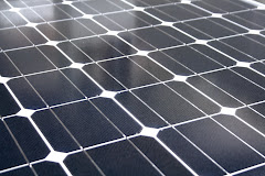
Advanced Solar Photonics (ASP) the cutting-edge developer of laser equipment for solar panel processing, thin-film solar cells, and commercial solar products presents the photovoltaic industry with Zero Width Laser Cutting Technology® (ZWLCT®). This process is a non-contact method which splits glass and other non-metallic brittle materials on the molecular level with tremendous speed, no material loss, and no chips or other debris associated with conventional scribe and break technology.
 Precisely cutting glass and other substrates has always been a vexing problem for the solar industry. For years now, there have been two major cutting methods: mechanical scribing or sawing and laser cutting. The explosive rise of the photovoltaic industry has put new demands on these existing cutting technologies. Advanced Solar Photonics utilizes ZWLCT® in its Fantom G8™, a thin-film laser scribing system.
"Zero Width Laser Cutting Technology® can be used for precise glass separation at production speeds not previously possible and with edge characteristics not attainable by any other process to date. The processed glass is four to five times mechanically stronger and has defect free edges without additional edge processing, said Edgardo Rodriguez, Vice President of sales for Advanced Solar Photonics. “Using this patented method aids the glass in withstanding extreme day/night temperature changes in the harsh desert environments by maintaining the integrity of the glass, thus strengthening it and ensuring long term stability.”
Zero Width Laser Cutting Technology® produces the maximum MicroCrack depth in the subsurface layer of the glass and not thermal-fracturing of the glass. After performing this application, the human eye is unable to see any change in the properties of the glass; however, when applying a small amount of pressure, the glass will split along the scribe line. Following the split, the glass has no particular damage and the highest edge quality which one can safely run their finger over requiring no further processing making grinding and cleaning lines unnecessary."
About Advanced Solar Photonics
Advanced Solar Photonics is the cutting-edge developer of laser equipment for solar panel processing, thin-film solar cells, and commercial solar products for the solar industry. Our laser equipment performs edge isolation, deletion, glass scribing, coating removal, laser marking and cutting. Our thin-film solar panels are produced using our proven patented method and expertise gained first hand to manufacture panels with one of the highest thin-film efficiencies and low cost per kilowatt hour. Additionally, ASP has created commercial equipment, like the solar tower, utilizing our thin-film panels. Our various technologies can increase production and efficiency, minimize waste, and in some cases, increase the overall efficiency of the PV cells. For more information, visit http://www.advancedsolarphotonics.com/ or call us direct at (407) 829-2613.
Advanced Solar Photonics is the cutting-edge developer of laser equipment for solar panel processing, thin-film solar cells, and commercial solar products for the solar industry. Our laser equipment performs edge isolation, deletion, glass scribing, coating removal, laser marking and cutting. Our thin-film solar panels are produced using our proven patented method and expertise gained first hand to manufacture panels with one of the highest thin-film efficiencies and low cost per kilowatt hour. Additionally, ASP has created commercial equipment, like the solar tower, utilizing our thin-film panels. Our various technologies can increase production and efficiency, minimize waste, and in some cases, increase the overall efficiency of the PV cells. For more information, visit http://www.advancedsolarphotonics.com/ or call us direct at (407) 829-2613.