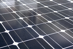
 As the solar industry moves towards the abundant and cost effective thin-film panels it is increasingly necessary to develop equipment capable of processing the largest solar panels possible. Although thin-film is the most inexpensive it is also is the least energy efficient. This has lead to the exponential increase in substrate sizes. Researchers have found that a ten times increase in substrate area only results in a 2.5 times increase in equipment costs. Advanced Solar Photonics not only offers standard equipment for marking, etching, scribing and edge isolation of smaller silicon solar panels but is now developing systems and equipment to process up to an eight foot (G8) thin-film solar panel.


6 years ago


No comments:
Post a Comment